Wednesday 8 November 2017

Everything You Need To Know About PCB Manufacturing!

The demand for PCBs (printed circuit boards) will seemingly not decrease in the near future; futuristic mobile phones, BluRay disc players, plasma TVs, electric cars have all made certain of this. PCB manufacturing technology is also not relenting and is up to date with modern electronic goods requirements. As an electronics manufacturer, we simply cannot be ignorant of modern PCB tech - the varieties of PCBs being as many as they are representative of the numerous modern PCB techniques and processes only recently developed. The design and manufacture of PCBs should be left to companies equipped with the latest of PCB equipment used in the prototyping and actualization phases.


PCB manufacturing can be divided into manufacturing the boards with or without components. Blank PCBs can be single or double-sided. Different PCBs have different capacities. We can have multilayered PCBs manufactured via techniques such as PCB milling, copper etching, screen printing etc. Most PCB fabrication companies also offer prototyping services - this involves developing a working PCB model before actual mass production can commence.

The raw materials used in PCB manufacturing are varied but copper is the basic material. Copper is always coated using a tin-lead combination to protect it against oxidation. The industry standard for PCB contact points is copper covered with this lead-tin combination, plated with nickel, and finished off with gold to maintain excellent conductivity. The quality control considerations that the manufacturer works by are a point to look out for. This involves the various visual as well as computerized scrutinies of the printed circuit board manufacturing steps from the conception to shipping stages. It also details the steps taken to rectify flaws and faults in the process.

PCB board manufacturing can be a very harmful process both to humans and the environment. This is especially so where the element Lead is present. A PCB manufacturing plant should be able to clearly define the safety considerations it has in place to deal with toxic matter, ways of disposing of obsolete PCBs, the recycling processes, and the modern human and environmentally-friendly equipment and processes they have in place.

The manufacturing process deployed is crucial as the working of the PCB and therefore the different equipment used in PCB manufacturing are complex and sensitive. The fabrication environment is also a controlled one so as to prevent the PCBs from any contamination. Your PCB firm of choice should be able to guarantee this even for the final product packaging process. Ignoring this is equal to putting your company and its electronic products' reputation in jeopardy. When partnering with a PCB manufacturer, it is important to choose a firm with extensive experience. As a customer, you should also be verifying if the firm has a proven track record.

Wednesday 20 September 2017

What is PCB and what is the use of PCB layout?

PCB stands for ‘Printed Circuit Board’ and it is used for high volume production without an expensive environment. Its main use is to connect the electronic components manually. PCB products are used in simple electronic products and are best used to connect electronic components using constructive tracks onto a non-conductive substrate. PCB can be of different types - single copper layer, double sided copper layers, or multi-layers which will have outlet & inner layers. What does it do? They allow higher component density in the primary insulating substrate.

What is PCB Fabrication?

First, the designing of the PCB is done and a prototype PCB plays a critical and significant role in the creation of its design and manufacturing. Also, if there is any problem in the designing phase or if any changes are necessary for the design of the PCB prototype, then it can be done easily. A fresh prototype is created and supervised in case of any failure during the overall procedure. The entire process of PCB fabrication includes steps like - etching, multi-layer processing, masking, drilling, engraving photos, finishing and finally electrical testing.

PCB Testing

PCB testing is done to check the efficiency of the board and the test plays an important role in the completion of the process. To make the PCB function well and perform outstanding well, it used different types of specifications like Arlon using for longer life in high temperatures and for flexibility, polyimide is used. Has the test turned out to be negative? Replace or repair the entire board effectively. It will help incorporating advanced circuits to exhibit at PCB.

Prototype PCB Manufacturer


Provided here are some of the efficient tips in the PCB Layout

PCB layout ensures that the prototype PCB is functional after the fabrication process. The process gets neglected due to most of the attention of circuit formation. Consider the tips for improving the efficiency of the PCB layout –

Sizzling Traces: It is used in PCB assembly for higher resistance and the two points connect within the PCB. With the use of length, width, and thickness, the resistance of the trace is controlled.

Make Smaller Loops: Larger loops are made small as smaller loops have lower inductance. It spikes the result from a PCB, with reduction of an amount of higher frequency voltage.

Decouple Capacitor Placement: If the capacitor is placed near the power and ground pins, it results in an increase of efficiency.

Keep Noise Traces Away from Analog Traces: The doubling of the signal on the traces are the result of the placement of 2 types of traces.


There are many prototype PCB manufacturer who develops efficient circuit boards. These manufacturers are known for developing prototypes which serves the best interest in getting the fault-free final product.

Tuesday 12 September 2017

Facts You May Not Know About Print Circuit Boards!

It has been well established that prototype printed circuit boards are a very complex puzzle in themselves. Their usage is of a variety and they come in different sizes that depend on the use of it. And one thing is fixed for it, that it’ll always be an amalgamation of different components to come together for its assembly. 

Putting all these parts together can be a bit time taking and complex but we can break it down into the most common components to further understand its uses.


If you’re familiar with the purpose of prototype printed circuit boards or PCB fabrication, you probably know how commonplace and necessary they are in today’s technologically dependent world. But even though printed circuit boards are found in almost every device we use on a daily basis, you might not know these four amazing facts about PCBs:

1.Some gramophones had printed circuit boards.

If you come to think of it, prototypes PCBs aren’t something that is entirely a new concept. They were there is early 1900sand after that too. And they were used in a few gramophones and also tube radios. They might not look similar to the printed circuit board prototypes that we are used to seeing now, but no matter what the format was, they helped in bringing entertainment and new developments into our homes like they do today.

2.The first PCBs were funded by a music printing company.

Father of the Modern Printed Circuit Board, Paul Eisler escaped the Nazis, and he was an inventor from Australia. He worked at a music printing company and shared the idea with everyone of a new invention.  And that was to make the first printed circuit board prototype. So, the company decided to invest in his idea. Today we see the results of his hard work as the prototype printed circuit boards.

3. No one knows why they’re still green.

The green material that is used on the layout of the PCB is a solder mask that’s visible through the glass. But nowadays technology has improved; solder masks are available in various colors. But the question remains that, why is the board still green then? Some people believe its story goes back to the military reigns and some also say that unlike that belief it was just about being uniformed. The companies just wanted stick to their idea of convention and continue with the original color. But then the legacy does continue and we stick to have the color green with us till date. 

4. PCBs are vital in space travel.

Not a lot of people would know this, but as being an integral part of NASA’s space program, these circuit boards did help in getting the Apollo 11 astronauts to the moon and back safely. These boards are ideal for difficult electronics, given that they are light weight and need a very small amount of energy.  

Although we live with an assumption that the technology we see and use today is brand new, the fact remains that they go long back in time and have a very fascinating history to them.

Thursday 7 September 2017

How Printed Board Circuit works and how to get an efficient PCB layout?

Printed circuit boards are used in simplest electronic products and it connects electronic components using conductive tracks, pads and other features onto a non-conductive substrate. Advanced PCBs contain components embedded in the substrate and components are generally soldered on the PCB. It can be single sided which contain one copper layer, double sided which contain two copper layers, or multi-layers which will have outlet & inner layers. Multi-layer PCBs allow higher component density and FR-4 glass epoxy is the primary insulating substrate.


In simple terms, a PCB can be defined as a tool providing mechanical and electronic connections by routing signals & power. Before PCB, there used to be a wire-to-wire connection but the durability of the device can be problematic. With the increase in demand, these assemblies have become common now. Also, the use of smaller ubiquitous technology has made the system more cost-effective. PCB assemblies have an application in almost every electronic appliance like computers & printers, TVs, home appliances, digital clocks, and cell phones.

Tips and Tricks for an Efficient PCB Layout

The PCB layout is often neglected with the majority attention on the formatting of the circuits. It ensures that the prototype PCB is functional after the fabrication process. Look at some of the tips to improve the efficiency of a PCB layout –

Sizing Traces

A copper rack used in PCB assembly is high in resistance and it connects two points within the PCB. The resistance of the trace is controlled by designers with the use of length, width, and thickness. To provide different levels of thickness, designers use anything between one and six ounces of copper.

Make the Loops Small

Smaller loops have lower inductance and resistance and so large loops are made small as possible. The reduction of an amount of high-frequency voltage spikes results from a PCB with high loops.

Decoupling Capacitor Placement

Increase the efficiency by placing the capacitor near to the power and ground pins of integrated circuits. The placement of capacitors at a distance results in a reduction of inductance ability.

Keep Noise Traces Away from Analog Traces

The placement of 2 types of traces will result in doubling of signal on the traces. Now those of you are not looking to keep the noise on the need to keep the high frequencies away.

Leave Room

Prevent the shock hazards by leaving the room between copper traces and fills. There should be a proper distance between the two if solder mark is not working as a reliable conductor.

Contact the PCB manufacturer for the effective design and preparation of rigid flex PCBs. PCBs are having high density to support new products and small packaging. Also, it has extremely thin feature if a circuit board reduces the bias force with a thin base pill. Also, flexible PCB has a high thermal transfer feature and it is resistant to heat. The most highly heat resistant FPC has reached 150 degree Celsius and reached a maximum temperature at 175 degree Celsius.

Friday 11 August 2017

PCB the Soul of Contemporary Electronic Device!

There are hardly any devices which do not use the PCBs in contemporary time. A PCB is a thin board made of fiberglass, composite epoxy, or other laminate material. Conductive pathways are etched or "printed" onto the board, connecting different components on the PCB, such as transistors, resistors, and integrated circuits. Electronic components are usually placed by machine onto a finished PCB that has solder dabs in place. The PCB bakes in an industrial oven to melt the solder, which joins the connections. It is found that the most PCBs are made from fiberglass or glass-reinforced plastics with copper traces.

Use of the PCBs in the computer, laptop and many other devices-

PCBs are normally used in both desktop and laptop computers. They serve as the foundation for many internal computer components. There is the use of the PCB in the video cards, controller cards, network interface cards, and expansion cards. These components, all connect to the motherboard, which is also a printed circuit board.


Read Also:- PCB Providing Wiring of Socket Components in an Electronic Device!

The PCBs are widely used in many other electronic devices besides the computers and laptops.  The common household appliances like TVs, radios, digital cameras, cell phones, and tablets include one or more printed circuit boards. The PCBs, which are used in mobile devices look similar to those found in desktop computers and large electronics, but they are typically thinner and contain finer circuitry. PCBs can be single-layer for simple electronic devices. Printed circuit boards for complex hardware, such as computer graphics cards and motherboards, may have up to twelve layers.

PCBs are of following two types. Let’s compare them- 

  • Single layer PCBs- The single layer board is the least complex option and includes a one-sided layer of substrate. This board is built with the electrical components and parts attached to one side and on the other side there are the copper traces. The copper is used due to special reasons because it is a great electrical conductor. This copper layer is usually protected by a special solder mask. There is the silkscreen coating is a further feature to help mark the different components on the board. It is a useful board for the most basic electronics and will be used by the at-home hobbyists in their first electronics projects. This kind of board is relatively low-cost to PCB Manufacture compared to the multilayer. This simple designing is the reason it has plenty of limitations and is far from being the most used in the industry.


  • Multilayer PCBs- Now we come to the multi layered boards which are built with two or more layers. These layers are separated by insulation. The standard size is in the region of 4 to 10 layers, even though there are boards with up to 42 layers. This is type of boards are preferred very much, especially for the most complex electronic configurations. The different boards are connected using wires passing through the individual holes. Space and weight of these boards are lesser than the single layer boards. These boards are used in handheld devices, space probe equipment, medical machinery, servers and computers widely.


Wednesday 31 May 2017

Printed Circuit Boards Brought Drastic Change in Today’s Machinery!

Humans have shown extensive progress and have lifted themselves from the violent animal to civilized persons. Machines played a very vital part in doing so. Machines make our work easier and they reduce effort and time greatly. We are surrounded by the machines these days and most of our work is done by machines or by the help of the machines. There is constant up gradation in the technology of machines and new, faster, reliable and technologically superior machines are coming into the market. Most of the machines these days are electrically operated, for example computer. It is a very essential device which is used by almost every office no matter; it is private organization or government offices. We cannot imagine the human existence this time without the help of the machines. 


Printed circuit board solved problems of the conventional circuits as they rarely got short circuited -

In the past, the conventional circuits were used for making wiring in the machines. There used to be the protracted process of point to point wiring. For the big machine this wiring used to be very messy and wire junction used to get damaged while operating the machine for long time. These frequent short circuits used to cause early damage of the insulation of the wires. The insulation used to crack due to short circuits. Printed circuit boards gave the perfect solution of this problem. In the past, electronic devices used to fill large space and this used to make it very uncomfortable to move them. The printed circuit boards drastically help in reducing the size of the electronic devices.

The composition to better understand the printed circuit board -

The printed circuit board is a sheet and on this sheet which provides the platform to connect the components, the integrated circuits are attached. The thin strip of the conducting material which is copper in most of the cases is fixed to the sheet, and this sheet is attached with the insulated bottom sheet. The components are connected by this thin strip of conducting material. The metal is known as the Solder which connects the electrical components to the printed circuit board surface. The insulating sheet imparts the required mechanical support and strength to this board along with it; this makes the safe, secure connection among components easy by the conducting material. This circuit is slim in structure and this kind of coating mold this whole circuit in a single object.

Manufacturing of these printed circuit board circuits and their use in various machines -

Theses printed circuit boards are very helpful and are replacing the old and conventional circuits. They are widely used in many devices like TV, led screen, devices which are used in hospital, offices, etc. The printed circuit boards have created a kind of revolution because these circuits are reliable and last very long. There are various manufacturing companies which are making these circuits for the different devices and embedding these circuits in the various devices.

Friday 14 April 2017

DESIGN AND MANUFACTURE OF PRINTED CIRCUIT BOARDS WITH SPCP

With the advent of modern computer and electronic technology, the Printed Circuit Board i.e. the PCB has become a very important component of all the electronic gadgets; either they are put to use domestically or industrially.  Not only PCBs are used in electronic connection making but are also act as the physical supports to various other electronic components to make them work as a single unit.


What is PCB: It is a thin plate upon which electronic chips and other such components are put on and placed so that the connection between the components could be made. Computers and laptops have non-singular number of boards, which are generally known as electronic cards or adapters. Circuit boards have two major categories:

Motherboard: It is the primary board that contains connectors for connecting devices to the main data bus. Characteristically, the mother board has CPU, memory-components, and essential regulators for the organization of the device. 

Expansion board: These are those boards which get plugged into the expansion slots of computers. They include other daughter cards, controller boards and network interface cards as well. 

Daughter card: It is that board which attaches directly to another board.

Controller board: They are special type of expansion boards which have controllers for nonessential devices to be connected to a computer which one frequently needs to add.

Network Interface Card: These are those expansion boards which enable a PC to be connected to a local-area network. 

From prototype to series production by SPCB Ltd:

They are world’s leading manufacturers of printed circuit boards; providing electronics developers printed circuit boards in all traditional as well as innovative technologies such as system solutions etc. Dozens of new circuit board designs go through their production facilities every day. They work from the very basic idea for a system within the span of development projects, to even samples and prototypes of the PCBs producing in medium and big volumes. This way, they are able to cover the whole manufacture series of the electronic applications. They provide printed circuit boards in the following single- and double-sided technologies:

• Multilayer
• Flex-Rigid
• Signal Integrity
• Thermal Management
• Wirebonding
• Embedded Component Technology
• Printed Polymer
• SMD Stencil

They act as personal contact person for their clients, by providing their printed circuit board specialists for on-site support to complete the realization of the clients’ products. In addition, clients also have the option of calculating and ordering printed circuit boards to be employed in various technologies; from their online shopping portal.

Thursday 23 March 2017

PCB Prototype Manufacture: the Easy Way with SPCB!

SPCB is a full service PCB manufacturer having specialization from quick turn prototypes to medium production volumes. This organization manufactures quality PCBs at a low cost to its global customers through on timely delivery. Their business goal is to be the most-cost-effective PCB manufacturer for prototyping and low-volume producer to work in the world. They commit themselves to meet the needs of their customers in terms of quality, delivery, cost-effectiveness and also any other demanding requests. As one of the most experienced PCB manufacturers in the world, they strive to make R&D work easy and hassle-free.


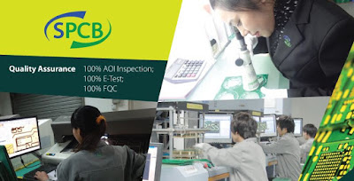
Quality: At SPCP, all the boards go through the toughest tests other than the usual basic visual checks. They have adopted most of the latest testing and inspecting equipments currently in use in the industry, such as Flying Probe Tester, X-Ray Inspection Machine, and Automated Optical Inspection (AOI) Machine. They have a dedicated team of new engineers from all around the world for creating new and tougher testing methodologies.

Fair-Price Policy: SPCB’s pricing structure is quite transparent and has no hidden costs. Their price is one of the most competitive in the world, and is just a small fraction of what other fabricators normally charge. Even many sensitive-to-prize customers like students and hobbyists hugely rely on them for their PCB prototype manufacture, for low-volume fabrication and assembly requirements. They try their best to save you money and time.

Customer Service: At SPCP all the orders receive a free engineering file review service from their professional technicians before the customer pays. Whenever customers have any problems, SPCP can always be reached via a live customer service executive to respond to mails or messages. Their service-executives follow the orders from the time customer submits the file to the minute he receives the PCBs and assembled PCBs in a satisfactory way.

Customer Friendly Return and Refund Policy: In case, dissatisfaction occurs due to the PCBs or assembled boards being non-usable due to the fault on SPCP’s part, customers can always ask for compensation. They shall either make refunds directly to customers’ account or credit the transaction-account; which shall be available to pay for the next orders with SPCP. There is also the option to rework the unusable boards or re-fabricate the PCB and re-ship to customer at their cost.

With these entire customer friendly policies and the manufacturing expertise, SPCB is the best in market prototype PCB manufacturer.

Wednesday 8 March 2017

Multilayer Printed Circuit Boards- The Next Big Thing to Your Business!

This is a hi-tech era where net and tech is at its highest peak. The best form of technology advancement can be seen in the form of Multilayer Printed Circuit Boards. These are the prototype circuit boards fabricated for a variety of different applications. Multilayer PCBs range from two to six layers.


Why To Use Multilayer PCBs?

If your business revolves around the latest technology, you are in extreme need to make use of latest applications and Multilayer PCB is one of the most needed technologies of today’s time. 

Though the use of these boards is not new to the phenomenon; it has been around us for centuries, it has got a huge hype in the recent years. It is so because the latest advancements used in the fabrication of these boards make them an efficient and indispensable need for almost all types of businesses that toy with electronic components. 

Small to midsized companies that wish to upgrade their businesses with the advanced technologies but can’t afford to pay a substantial amount can also get benefited from the loaded features of Multilayer Printed Circuit Boards provided that they count on a company that deals with providing high quality PCBs at much affordable price.

• There are several fine features about relying on a company that focuses on manufacturing a multilayer PCB for small to medium sized companies.

• The first and foremost feature about relying on such a company is that if you want to buy PCB in less quantity, you can easily get it from such companies.

• Secondly, you can get a prototype design that is specifically fabricated for you keeping your particular specifications in mind.

• These companies work with you in order to give you the same what you are looking.

• Last but not the least, these companies provide you high quality PCBs at cost effective price. 

If you are not sure which company to count on to get all the above said features in terms of your Multilayer Printed Circuit Boards, you can simply have faith in the unmatched service and products of “SPCB”. Relying on a PCB manufacturing company that deals with designing and making all sorts of printed circuit board for a all types of businesses will bestow you with a product that is the next best thing that is handmade, without giving extra burden to your pocket.

Your business can be highly benefited from the high technology when it comes to the multilayer PCB at an affordable cost.

Friday 10 February 2017

Advantages of a Double Sided PCB

A double sided PCB is used widely. It comes with 2 sided traces, a bottom and top layer. If you have a PCB that has double side traces but the electronic components are on one side this is also a double sided one but the assembly has been done differently. This kind of PCB is seen quite commonly in prototype and production circuits. They are used because they make laying tracks easy and increase the density of components. These PCBs are made of a non-conductive material as the substrate just like you see with regular circuit boards. Over the substrate comes a copper layer and with a double sided one, this copper layer goes on the top and bottom side as well. There are advantages of using this type of PCB as follows:

• Density of components–

Since they have a full extra layer one is able to add more tracks that will then connect to the components on the other side.  With space freed up, you can place more components and put them close together or you may decide to have extra connections.

• Increased heat dissipation–

When you decide to use these double sided boards, you will realize that heat dissipates more because of the extra copper layer. This is achieved during the process of etching by removing just the copper needed to allow for track creation. Instead of removing the extra copper, leave it in place to help dissipate heat.

Printed Circuit Board Services


If you are considering the use of a double sided PCB you should do it carefully because the production of the board will be more complex and once it has been assembled it will need delicate handling. You also need to consider the costs that are associated with making this type of board vis a vis a single sided PCB. In fact, the cost of manufacturing is usually the biggest consideration for most people because the manufacturers will ask for more money in order to process the second side. This cost will include solder mask, etching, and component layout.

If you are looking to add your own custom considerations, then you can expect that you will be charged for the process of designing the board. The manufacturer wants to make sure that you will be pleased with the end product, one that functions well and avoids the various issues that affect high speed and analog digital circuits such as parasitic capacitance and inductive losses.

In summary, with a double sided board you can expect to enjoy more design flexibility, a higher level of complexity in the circuit, increased density, lower costs and a smaller board size since you will be using both sides and not just one. With all these benefits, it is no wonder that the double sided board continues to be the most widely used component for multiple applications.

Wednesday 18 January 2017

Significance of Halogen-free Printed Circuit Boards in Real World

A Printed Circuit Board, also referred to as Printed Wiring Board is an important cog of electronic equipments which is comprised of thin strips of a conducting material for instance “copper”. The PCBs are developed by deploying and utilizing many compounds as well as elements for a variety of purposes.

What Led to Halogen-free Formula?

During the initial days of PCB development, certain toxic compounds were used in its making for utilizing the specific, useful feature of that element or as a cost-saving aspect of manufacturing. To overcome this threat the skilled souls evolved the formula of “Halogen-free PCB” which are devoid of any toxic elements and have the power to serve the similar purpose without posing any threat to the universe.

Now let’s learn how the elements of Halogen family can cause a serious threat to the world, and how halogen-free PCB holds its worth in the advanced, real world.


Read Also: Printed Circuit Board –Its Composition, Functions and Applications!

PCBS That Comprise Halogen 

Common compounds that are taken under use into the process of PCB development –belong to the family of Halogen elements. These elements are Chlorine, Flourine, Bromine, Iodine and Astatine etc. The composition of PCB using all such elements provides certain benefits to the electronics that use it; however, they are quite harmful to human life in one way or another.

With the development of the world and humanity, an increased awareness of the threats through those materials and elements was found which lead manufacturers seek substitute methods and find new materials that don’t pose a threat to humans working with such devices.

How Are Halogen Elements Harmful?

While the debate on the toxicity of halogens within PCB development continues, there are two chief elements which compose the general consensus of a halogen-free circuit board –chlorine and bromine respectively. Each accomplishes a specific purpose in the overall functionality of electronics but also pose a threat to the continuity of life for humans, animals and nature.

Chlorine: Continued exposure and dangerous concentrations of chlorine can cause cruel complications such as pulmonary edema, consistent fluid in the lungs, and developing asthma in kids and preschoolers. Chlorine is that toxic element that can be a threat to human life, and can cause severe damage to an eco-system.

Bromine: Being another component used in the making of Printed Circuit Board, bromine can cause kidney failure as well as brain damage due to systemic poisoning. Moreover, sustained exposure to bromine can result in the drop of blood pressure to intolerable levels for internal organs, assisting in overall physical dysfunction. For those that continuously breathe in bromine, there are chances of long-term lung diseases up to varying degrees.

Halogen-free PCB

As halogen and its constitutes pose a threat to the world, halogen free PCBs would be an ideal solution for not only one but many problems and threats. The toxicity that is created from the elements of halogen family (such as chlorine & bromine) could put individuals and eco-systems in great jeopardy. Apart from precious metals such as copper, aluminum etc, choosing a halogen-free product in manufacturing PCBS can keep the developers, future technicians and individuals safer from experiencing health complications due to considerable exposure.

Halogen-free PCBs are the specialty of certain advanced Printed Circuit Board services which think not only of the technology and electronics, but also of the humans, nature and the world.